
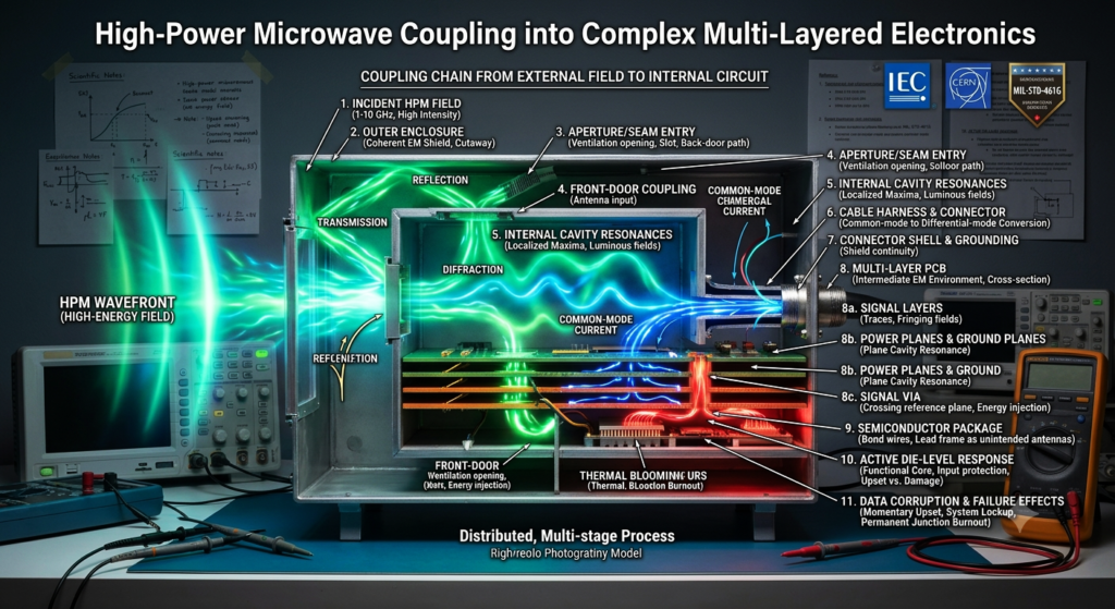
High-power microwave coupling into modern electronics is frequently described as though an external electromagnetic field simply reaches a circuit board and deposits energy into its components, yet the actual interaction is a distributed, multi-stage process in which the incident field encounters an entire hierarchy of conductive structures, dielectric materials, openings, cables, antennas, connectors, shielding interfaces, printed-circuit layers, power-distribution networks, semiconductor packages, and internal interconnects before any resulting disturbance reaches the functional core of the system. Each layer modifies the field through reflection, transmission, diffraction, resonance, conversion between common-mode and differential-mode currents, and redistribution through the electrical network, which means that the disturbance arriving at a sensitive device can differ greatly in amplitude, waveform, duration, phase, and spectral content from the field outside the equipment.
The term coupling refers to this transfer of electromagnetic energy from an external or internal source into an unintended electrical path, while high-power microwave coupling refers to conditions in which the transferred energy may exceed the tolerance of ordinary electromagnetic-compatibility design and produce effects ranging from momentary data corruption to permanent physical damage. The International Electrotechnical Commission addresses this broader problem through standards for intentional electromagnetic interference and high-power electromagnetic environments, while the United States Department of Defense electromagnetic-interference standard MIL-STD-461G establishes conducted and radiated susceptibility requirements for military equipment and subsystems, reflecting the engineering reality that susceptibility must be evaluated across the full equipment architecture rather than inferred from the tolerance of an isolated semiconductor.
High-power microwave exposure can take different forms, including comparatively narrowband radiation concentrated within a limited spectral region, broadband transients containing energy across a wider range of frequencies, repeated pulses that interact with recovery and protection times, and longer-duration fields that create sustained electrical or thermal stress, although the practical effect of any such environment depends less on the external label assigned to the waveform than on how efficiently the equipment converts the arriving electromagnetic field into internal voltage, current, and dissipated energy. A large external field may produce a relatively modest internal disturbance when the enclosure, interfaces, cables, and filters work together as a coordinated protective boundary, while a lower external field may create a serious internal response when it aligns with an enclosure resonance, enters through a connected antenna, excites a long cable harness, crosses an inadequately bonded seam, or reaches a high-impedance node that requires little injected charge to change logical state. This dependence on geometry and system state explains why susceptibility cannot be represented by one universal threshold, since orientation, polarization, frequency, cable configuration, connector condition, enclosure assembly, operating mode, processor activity, software state, temperature, component aging, and attached peripheral equipment can all change the final response. The IEC high-power electromagnetic effects report for civil systems identifies the growing use of digital electronics as a reason for concern about upset and damage in severe electromagnetic environments, while IEC 61000-4-36 provides a framework for deriving immunity test levels and selecting practical test methods for equipment and complete systems exposed to intentional electromagnetic interference.
The Coupling Chain from the External Field to the Internal Circuit
The first major distinction in high-power microwave analysis is commonly expressed through the concepts of front-door and back-door coupling, with front-door coupling referring to energy entering through a structure deliberately designed to receive electromagnetic signals, such as an antenna, sensor aperture, radio-frequency port, or communication interface, while back-door coupling refers to unintended entry through enclosure openings, seams, ventilation paths, cables, power conductors, connectors, displays, control lines, structural joints, and other features that were never intended to function as receiving antennas. The distinction is useful because an intentional receiver can collect and concentrate electromagnetic energy efficiently within its operating region, after which the coupled signal may pass through matching networks, filters, amplifiers, limiters, mixers, or converters that were designed for ordinary signal levels rather than extreme incident power, while back-door coupling tends to depend more heavily on accidental geometry, imperfect shielding, common-mode currents, and resonance within the surrounding structure.
Real equipment often experiences both paths simultaneously, since an external field may enter through an antenna port while also inducing currents on the chassis and cable harness, after which the two disturbances interact inside the receiver, power supply, or printed-circuit assembly. Research on the joint analysis of front-door and back-door electromagnetic coupling and broader reviews of electromagnetic environmental effects emphasize that complete susceptibility assessment must include antennas, shells, cables, openings, and internal circuits rather than treating either coupling path as the sole mechanism.
The outer enclosure is the first protective layer for many electronic systems, although its performance depends on the entire assembled boundary rather than the nominal conductivity or thickness of its largest metal panels, since current must flow continuously across joints, fasteners, access doors, removable covers, connector panels, ventilation openings, windows, and cable penetrations if the enclosure is to behave as a coherent electromagnetic shield. Even a highly conductive enclosure can lose substantial effectiveness when seams develop excessive impedance, conductive coatings are interrupted, gaskets are compressed unevenly, fasteners are widely spaced, paint or corrosion isolates mating surfaces, or openings support field penetration at particular frequencies. Apertures also interact with the internal cavity, which means that the energy admitted through a slot or hole may excite resonant field patterns and create localized internal maxima rather than distributing uniformly throughout the enclosure. The internal field can therefore vary sharply from one point to another, and a component positioned near a cavity maximum may experience a stronger disturbance than another component only a short distance away, even though both are housed behind the same exterior wall. The National Institute of Standards and Technology has developed reverberation-chamber methods for measuring the shielding effectiveness of physically small but electrically large enclosures, including configurations with circular apertures, while additional NIST research on nested reverberation chambers demonstrates that material behavior must be interpreted together with aperture and cavity effects.
Complex systems rarely contain only one enclosure, since a vehicle, aircraft, satellite, industrial controller, communication terminal, medical platform, or data-processing installation may place circuit cards inside modules, modules inside racks, racks inside rooms, and rooms inside a larger facility, with every boundary providing some attenuation while also introducing new penetrations and resonant volumes. This nested structure creates a multi-layer coupling problem in which the field that penetrates the facility wall excites currents on internal cable trays and racks, the rack field enters equipment housings through connectors or ventilation paths, the equipment field couples onto board traces and power planes, and the resulting circuit disturbance propagates through semiconductor packages and internal device structures. The attenuation associated with these layers cannot always be multiplied as though each barrier operated independently, because cables and structural conductors may bypass one or more boundaries, common grounding networks may carry current between compartments, and resonant interactions may increase the field at selected locations. A system can therefore possess excellent shielding at the equipment enclosure while remaining vulnerable through an unfiltered power line that crosses the same boundary, or it can use shielded cables whose terminations introduce enough impedance to convert shield current into an internal signal. The latest edition of IEC 61000-5-6 addresses the mitigation of external electromagnetic influences at the facility and installation level, including high-power electromagnetic transients and intentional electromagnetic interference, while IEC TS 61000-5-10 provides protection guidance for commercial facilities whose critical electronics must continue functioning in severe electromagnetic environments.
Cables and wiring harnesses are among the most important coupling structures because their physical length allows them to intercept electromagnetic energy over a region much larger than an individual circuit component, after which the induced disturbance can be conducted directly into an enclosure through power, communication, sensor, control, or grounding interfaces. A cable does not respond only according to its nominal function, since its shield, signal conductors, return paths, connector shells, pigtails, backshells, and nearby structures form a distributed electromagnetic network whose behavior depends on routing, separation, termination, balance, and impedance. A field that initially produces common-mode current on the cable can be converted into differential voltage by asymmetry in the conductors, unequal connector impedances, imperfect shield bonding, or differences between internal circuit paths, allowing energy that appeared confined to the outside of the cable to reach a receiver input or power rail. Cable shields can reduce coupling substantially when they preserve circumferential continuity and are bonded correctly at the penetrated boundary, although a shield with poor termination can cease behaving as an extension of the enclosure and instead become part of the receiving structure. NIST measurements of high-frequency cable shielding effectiveness found that impedance mismatches and test configuration could change measured coupling by large amounts, illustrating why cable immunity cannot be inferred reliably from the presence of braided or foil shielding alone, while the NASA electromagnetic-compatibility design handbook treats cable shielding and termination as system-level design issues rather than optional additions applied after circuit development.
Connectors occupy a particularly sensitive position because they are simultaneously mechanical interfaces, conductive discontinuities, shielding penetrations, impedance transitions, and maintenance points, which allows small variations in assembly to alter electromagnetic performance throughout the life of the equipment. A connector shell that is bonded continuously to the enclosure can carry shield current around the protected interior, while a shell connected through a long wire or narrow trace introduces inductive impedance that encourages part of the current to enter the circuit reference structure. Filtered connectors can provide attenuation at a boundary, yet their effectiveness depends on grounding geometry, installation, parasitic behavior, and the spectral content of the disturbance, while optical-fiber interfaces can remove a direct metallic signal path but still require attention to conductive connector bodies, power supplies, transceivers, and openings through the enclosure. NIST work on the electromagnetic shielding characteristics of optical-fiber connectors demonstrates that replacing a copper data link with optical fiber does not automatically make the complete penetration electromagnetically invisible, since the bulkhead hardware and associated aperture remain part of the shielding problem. The broader principle is that every interface crossing a protective boundary must be treated as a controlled electromagnetic transition, with the mechanical, electrical, and shielding functions designed together rather than assigned to separate engineering teams after the architecture has already been fixed.
Coupling Through Printed-Circuit Layers, Packages, and Functional Networks
Once electromagnetic energy reaches a printed-circuit board, the concept of a single vulnerable trace becomes inadequate because a modern multilayer board contains signal layers, power planes, ground planes, dielectric substrates, vias, component lands, connector footprints, decoupling networks, clock trees, high-speed serial channels, analog sections, radio-frequency sections, and switching power circuits that interact as one distributed structure. Closely spaced power and ground planes can provide useful high-frequency return paths and distributed capacitance, yet they can also behave as resonant cavities whose internal field patterns are excited by vias, discontinuities, connector currents, or external radiation. Signal vias that cross reference planes can inject energy into the plane pair, while splits or gaps in a reference plane force return current to follow a longer path, increasing loop area and creating stronger conversion between intended signals and unwanted electromagnetic modes. Board edges permit fringing fields, and the relationship between layer spacing, dielectric properties, board dimensions, via placement, component loading, and decoupling determines where resonances appear and how efficiently they are damped. A study of radiated susceptibility in multilayer printed-circuit boards examined coupling into power and ground planes and the influence of perimeter via fencing, while research on multilayer PCB plane cavities and through-hole via excitation shows that vias can couple signal energy into the power-distribution structure and produce complex board-wide electromagnetic behavior.
The multilayer board therefore functions as an intermediate electromagnetic environment located between the enclosure and the semiconductor, with its own modes, attenuation mechanisms, conversion paths, and localized field concentrations, while the components mounted on it continually modify those properties through their package capacitance, supply impedance, input protection, clock activity, and operating state. An external disturbance coupled onto one part of the board may travel through the power-distribution network and reach many devices simultaneously, or it may enter a high-speed interface and propagate through receivers, serializers, clock-recovery circuits, and processing logic before appearing as a functional error far from the original coupling point. Decoupling capacitors, ferrites, filters, and plane structures can suppress disturbances within their intended regions, yet every real component possesses parasitic inductance, capacitance, resistance, and package resonance, which means that a protective network effective at one frequency may become less effective or even provide an unintended transfer path at another. The result is a layered transfer function shaped by the board geometry and the component network, while high-power excitation adds nonlinear behavior because protection devices conduct, semiconductor junctions change impedance, power converters enter current limiting, and local heating shifts component characteristics. Research on intentional electromagnetic interference in power electronics identifies field-to-cable and field-to-board coupling as central susceptibility paths, while also noting that saturation, thermal effects, and component aging can influence system performance and deserve consideration beyond immediate pass-or-fail testing.
Semiconductor packages add another layer between the board and the active device, since bond wires, lead frames, solder balls, redistribution layers, package substrates, heat spreaders, exposed pads, and internal power networks can behave as unintended antennas, inductive loops, capacitive injection paths, and resonant interconnects. The package may attenuate part of the board-level disturbance while concentrating another part onto a supply pin, signal input, substrate connection, or protection structure, and advanced packages containing several dies, stacked memory, chiplets, interposers, and embedded passive components create multiple internal paths that cannot be represented accurately by a simple lumped model at microwave frequencies. At the die level, the disturbance can enter through input and output protection structures, power rails, clock networks, substrate coupling, analog bias circuits, memory cells, or internal interconnects, after which the response depends on device technology, logic state, supply voltage, temperature, timing, and the duration of the induced transient. Modern low-voltage digital circuits can change state in response to relatively small disturbances at sensitive nodes, while their dense interconnects and fast edges provide many paths through which an injected event can spread across clock, reset, memory, and communication functions. The increasing density of advanced packaging also creates reliability concerns involving interconnect stress and latent degradation, as discussed in research on the reliability of advanced electronic packaging, although the precise response to a high-power electromagnetic event remains highly dependent on the package and system architecture.
The observable consequence of coupling can be classified broadly as temporary interference, recoverable upset, system-level lockup, protective shutdown, latent degradation, or permanent damage, yet these categories form a continuum rather than a set of sharply separated outcomes. Temporary interference may appear as increased noise, corrupted sensor readings, degraded communication quality, timing jitter, or false control inputs that disappear when the field is removed, while recoverable upset may require automatic retry, watchdog reset, software restart, or power cycling before normal operation returns. A more persistent event may alter memory contents, disrupt a boot process, corrupt stored configuration, damage a communication transceiver, or leave a protection device partially degraded, creating a condition in which the equipment appears functional after the event but possesses reduced margin against later electrical, thermal, or electromagnetic stress. Permanent failure may involve junction damage, dielectric breakdown, metallization damage, latch-up followed by excessive current, overheating in an input structure, or destruction of a power-conversion component, although the location of the visible failure may not identify the original entry path because energy can travel through several layers before being dissipated. The IEC immunity framework for radiated radio-frequency fields, conducted radio-frequency disturbances, and high-power intentional electromagnetic interference reflects this need to evaluate both the applied environment and the equipment’s functional response under defined operating conditions.
Software and digital architecture strongly influence the final system effect even though the initial coupling process is electromagnetic, since hardware errors are interpreted by processors, operating systems, control algorithms, communication protocols, and safety logic that may suppress, amplify, propagate, or conceal the disturbance. Error-detecting codes, redundant communication, watchdog timers, state validation, current monitoring, secure boot processes, and fail-safe control can convert a brief electrical upset into a controlled recovery, while poorly managed exception handling or a single shared dependency can transform a localized transient into a system-wide loss of function. Redundancy provides limited benefit when redundant channels share the same enclosure, cable route, power converter, clock source, grounding structure, or software fault, because one coupled field may affect every channel through the common element. A resilient architecture therefore separates critical functions electromagnetically as well as logically, distributes power and communication paths where practical, validates state after abnormal events, and ensures that recovery mechanisms themselves remain protected. These measures do not replace shielding, filtering, and grounding, although they reduce the probability that a residual disturbance crossing the physical defenses will become an uncontrolled operational failure. The NIST electromagnetic compatibility and smart-grid white paper treats electromagnetic compatibility as an integral design process for interconnected electronic systems, which is especially important where software, communications, sensing, and power electronics depend on one another.
Modeling, Testing, and Engineering for Electromagnetic Resilience
Modeling a complex multi-layered electronic system requires a hierarchical approach because no single simulation can efficiently resolve the external environment, facility structure, enclosure seams, cable harnesses, circuit-board planes, packages, and transistor-level behavior with equal fidelity across the full frequency and time range of interest. Large structures may be represented through full-wave electromagnetic models, transmission-line methods, network models, or statistical cavity techniques, while detailed regions such as connector penetrations, apertures, board sections, and package interconnects receive finer treatment, after which the resulting fields and currents are transferred into circuit simulations that evaluate functional response. This decomposition must preserve the dominant coupling mechanisms between scales, since a model that predicts enclosure field strength without representing the attached cable network can miss the main conducted path, while a detailed board simulation driven by an arbitrary uniform field can produce precise results for an unrealistic internal environment. Statistical approaches are valuable when electrically large cavities support many overlapping modes and small changes in frequency, position, or configuration produce large local variations, while deterministic models remain essential for known apertures, harnesses, and circuit paths. A Sandia National Laboratories systematic coupling methodology combines practical measurement and simulation to characterize propagation and device immunity within complex facilities, while NIST research on reverberation-chamber shielding measurements provides methods for assessing enclosures under statistically varied field conditions.
Testing must reproduce the relevant coupling path while controlling enough variables to make the result interpretable and repeatable, which is why electromagnetic immunity programs use several complementary facilities rather than relying on a single chamber or test configuration. Anechoic or semi-anechoic chambers support controlled illumination and polarization, transverse electromagnetic cells provide standardized fields for suitable equipment sizes and frequency ranges, bulk-current injection and conducted-immunity methods stress cable interfaces directly, reverberation chambers create statistically varied high-field environments, and direct injection can evaluate particular ports or circuit paths when the relationship to the external environment is already understood. High-power testing introduces additional concerns involving field measurement, pulse fidelity, chamber reflections, instrumentation protection, personnel safety, equipment state monitoring, and the possibility that cables connected to diagnostic instruments create coupling paths that would not exist in normal operation. The test object must also be exercised through representative operating modes, since an inactive input, sleeping processor, disabled transmitter, unloaded power converter, or disconnected peripheral may respond differently from the same hardware performing its intended function. IEC 61000-4-36 summarizes practical immunity test methods for intentional electromagnetic interference, while IEC TR 61000-4-35 addresses high-power electromagnetic simulators, including narrowband microwave facilities and wideband radiated-field systems.
Reverberation chambers are particularly useful for complex electronics because mechanically or electronically stirred fields expose the equipment to many effective illumination directions and polarizations, allowing engineers to characterize statistical susceptibility without manually reproducing every possible external orientation. Their usefulness does not remove the need for careful loading, field calibration, cable arrangement, and uncertainty analysis, since the test object and its supporting equipment alter the chamber response, while the location of internal resonances and coupling maxima changes with configuration. Direct illumination remains valuable when a specific orientation, aperture, cable, or antenna path must be studied, and comparison between methods can reveal whether a measured response is dominated by a deterministic feature or by the broader cavity environment. NIST has compared direct-illumination and reverberation-chamber shielding measurements and has also studied the effect of peripheral-equipment loading on reverberation-chamber metrics, reinforcing the principle that the test setup must be treated as part of the electromagnetic system rather than as a neutral background.
Protection begins with architectural zoning, in which the system is divided into electromagnetic regions with defined boundaries, allowable field levels, controlled penetrations, and coordinated grounding structures, so that each successive layer reduces the disturbance before it reaches increasingly sensitive electronics. The outer facility or platform provides the first boundary, internal racks and enclosures provide additional barriers, filtered and bonded interfaces control energy crossing between zones, cable shields preserve boundary continuity, board-level filters and reference planes reduce residual coupling, and device-level protection handles the remaining transient. This layered approach prevents any one protective element from carrying the full burden, while also allowing engineers to identify where attenuation is lost and where maintenance must preserve electrical continuity. Shielding materials remain important, although seams, apertures, joints, and penetrations often determine assembled performance, while grounding must be understood as the management of return current and reference structure across frequency rather than as the simple presence of a wire connected to earth. NASA’s bonding, grounding, shielding, and electromagnetic-interference standard provides system-level requirements for electrical and electronic ground systems, while the NASA spacecraft grounding handbook emphasizes that grounding architecture must be established early because later equipment-level grounding decisions must remain consistent with the system reference structure.
At the enclosure level, effective protection requires conductive continuity across joints, appropriate gasket materials, controlled aperture dimensions, filtered penetrations, bonded connector shells, suitable ventilation treatments, and maintenance procedures that prevent corrosion, paint, contamination, or mechanical wear from degrading the electromagnetic boundary. Honeycomb vents and waveguide-like penetrations can support airflow while reducing field transmission when designed for the relevant environment, although their performance depends on dimensions, conductivity, installation, and frequency, while transparent windows or displays may require conductive coatings or meshes integrated with the surrounding frame. Composite structures create additional challenges because their mechanical strength does not guarantee metallic shielding behavior, and joints between composite and metal sections may dominate current flow. NASA’s design guidelines for shielding effectiveness in composite materials address electrical characteristics that affect electromagnetic compatibility, while NIST measurements of advanced composite shielding materials demonstrate the need to evaluate real material and enclosure behavior through controlled measurement.
At the cable and interface level, resilience depends on minimizing exposed loop area, maintaining balanced signaling, routing conductors close to their reference paths, preserving shield continuity at boundaries, separating susceptible interfaces from noisy or exposed structures, and placing filtering or transient suppression where current crosses into the protected region. The physical placement of the protective device is critical because a filter connected through a long trace or wire allows the unfiltered section to radiate or recouple energy inside the enclosure, while a shield terminated through a narrow pigtail may possess enough high-frequency impedance to defeat the intended boundary. Optical isolation can remove direct conductive communication paths, although the associated transceiver power, enclosure penetration, and connector hardware still require protection, while transformer or galvanic isolation can reduce some common-mode paths but introduces parasitic capacitance that becomes relevant at high frequency. The correct strategy depends on the interface and cannot be reduced to a universal rule requiring every cable shield to be terminated in the same manner, since safety, low-frequency grounding, high-frequency shielding, corrosion control, and system topology must be reconciled within one architecture. NASA and NIST guidance on cable shielding and shield termination and measurement of cable shielding configurations provides a practical basis for this system-level treatment.
At the printed-circuit level, resilience improves when signal-return paths remain continuous, high-speed loops remain compact, power-distribution resonances are controlled, external interfaces are filtered near their entry points, sensitive analog or timing circuits are separated from exposed conductors, and the layer stack is designed as an electromagnetic structure rather than as a routing convenience. Via fencing, edge plating, controlled reference transitions, closely coupled planes, damping networks, local decoupling, and careful connector placement can reduce field penetration and board-level resonance, although no measure should be adopted solely from a generic checklist because its effectiveness depends on board dimensions, frequencies, component loading, dielectric properties, and the surrounding enclosure. The board must also be evaluated together with its cables and mechanical installation, since a layout that performs well on an isolated bench can respond differently after connection to a long harness, conductive chassis, display, antenna, or external sensor. The open-access study on PCB radiated susceptibility and via fencing provides a useful example of how board-edge treatment influences coupling to power and ground planes, while research on split reference planes in high-speed multilayer boards demonstrates how disrupted return paths can increase signal distortion, crosstalk, and radiation.
Protection must finally be verified through a lifecycle program rather than a single qualification event, because shielding joints loosen, gaskets age, connector shells corrode, cables are replaced, software changes, circuit cards are revised, commercial components become obsolete, and field repairs introduce configurations that were never represented by the original test article. Susceptibility can also emerge after an apparently minor design change, such as moving a connector, replacing a power converter, altering a board stack, changing a cable supplier, modifying a ventilation opening, or updating processor firmware in a way that changes timing and recovery behavior. Configuration control should therefore identify electromagnetic protection features as critical design elements, while inspection and maintenance should include bonding resistance, gasket condition, connector assembly, cable routing, filter installation, and enclosure integrity. Retesting may be required when changes affect coupling paths or functional response, while fault logging and post-event diagnostics should distinguish between transient upset, software failure, power-quality disturbance, and permanent hardware degradation. The European Space Agency electromagnetic-compatibility laboratory supports EMC testing and magnetic-cleanliness verification for complex space projects, while the DoD and IEC standards provide structured requirements for controlling emissions, evaluating susceptibility, and maintaining a reproducible basis for system qualification.
High-power microwave coupling into complex multi-layered electronics is ultimately a problem of system topology, since the external field becomes operationally significant only after it finds a path through the physical hierarchy and creates an electrical disturbance capable of changing system behavior. The enclosure, aperture, seam, cable, connector, board, package, power network, semiconductor, software state, and recovery architecture all participate in the final result, while the weakest element may shift with frequency, orientation, configuration, maintenance condition, and operating mode. Effective resilience therefore emerges from coordinated architecture, controlled boundaries, well-designed interfaces, continuous return paths, validated filtering, robust circuit layout, protected power distribution, fault-tolerant software, representative testing, and disciplined lifecycle maintenance, rather than from reliance on a single shield material or protective component. The most reliable engineering approach begins by tracing every plausible coupling route from the external environment to the critical function, measuring or modeling the transfer at each major boundary, testing the complete system in representative configurations, and ensuring that residual disturbances lead to controlled recovery rather than uncontrolled propagation through interconnected electronics. The continuing development of international HPEM immunity standards, facility-level mitigation guidance, military electromagnetic-susceptibility requirements, and advanced enclosure measurement methods reflects the growing recognition that modern electronics must be treated as nested electromagnetic systems whose resilience is determined by the integrity of the entire coupling chain.